|
| Place of Origin: | China |
| Brand Name: | OEM |
| Certification: | ISO9001 |
| Minimum Order Quantity: | Negotiable |
|---|---|
| Price: | Negotiable |
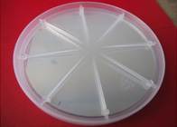
| Packaging Details: | 100g/bag or single wafer box packaging. |
| Delivery Time: | 5-7 working days after received your payment details working days after received your payment details |
| Payment Terms: | T/T, Western Union, L/C |
| Type/Dopant: | P/B | Orientation: | <100>+/-0.5degree |
|---|---|---|---|
| Size: | Dia4” X 0.5 Mm | Surface: | One Side Polished |
| Resistivity: | 2 ~ 4 Ohm-cm | Wafer Size: | 10 X 10 X 0.5mm 15x15x0.5mm ,or Other Size The Customer Request |
| High Light: | silicon substrate,silicon oxide wafer |
||
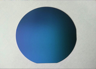
Pt/Ti/SiO2/Si single crystal wafer with Si Wafer and dia 4” x 0.5 mm
Typical Physical Properties of Pt/Ti/SiO2/Si single crystal wafer
|
Pt layer: |
150 nm |
|
Ti layer: |
20 nm |
|
SiO2 layer: |
300 nm |
Si wafer <100> P-type/B
dia4"x0.5mm SSP
Resistivity: 2 ~ 4 ohm-cm
we can cut the wafer into: 10 x 10 x 0.5mm 15x15x0.5mm ,or other size the customer request
![]()
Why choose us
1. Long history and high quality
More than 10 years experience in Chemcials industry. Design and manufacture high quality products with our qualified Lab.
2. Fast delivery and small order acceptable
Faster delivery by air or by express.(DHL,UPS ,TNT or Fedex). Small order is accepted, we treat every order well.
3. Wonderful team
Professional sales team to offer fast response within 24 hours and good service
Contact Person: Ms. Linda
Tel: +86-19945681435
Address: Rm 1712-1715, No.88, Sibao Rd, Shanghai , China